Mounter Terminology
(A~C)
Begins with the letter A
Accuracy: The difference between the measurement result and the target value.
Additive Process: A method of making PCB conductive wiring by selectively depositing conductive materials (copper, tin, etc.) on board layers.
Adhesion: Similar to the attraction between molecules.
Aerosol: Liquid or gaseous particles small enough to be airborne.
Angle of attack: the angle between the screen printing squeegee surface and the screen printing plane.
Anisotropic adhesive: A conductive substance whose particles pass current only in the Z-axis direction.
Annular ring: Conductive material around a drilled hole.
Application specific integrated circuit (ASIC special application integrated circuit): a circuit customized by the customer for a special purpose.
Array (array): A set of elements, such as solder ball points, arranged in rows and columns.
Artwork (wiring diagram): The conductive wiring diagram of the PCB, used to generate the original photo, can be made in any scale, but generally 3:1 or 4:1.
Automated test equipment (ATE): Equipment designed to automatically analyze functions or static parameters in order to assess performance levels, also for fault isolation.
Automatic optical inspection (AOI): On an automatic system, a camera is used to inspect a model or object.
Begins with the letter B
Ball grid array (BGA ball grid array): The packaging form of integrated circuits, whose input and output points are solder balls arranged in a grid pattern on the bottom surface of the component.
Blind via: A conductive connection between the outer layer and the inner layer of the PCB that does not continue to the other side of the board.
Bond lift-off: The failure to separate the solder pins from the pad surface (circuit board substrate).
Bonding agent: An adhesive that bonds a single layer to form a multi-layer board.
Bridge: Solder that connects two conductors that should be conductively connected, causing a short circuit.
Buried via: A conductive connection between two or more inner layers of a PCB (ie, invisible from the outer layers).
Begins with the letter C
CAD/CAM system (computer-aided design and manufacturing system): Computer-aided design is the use of specialized software tools to design printed circuit structures; computer-aided manufacturing converts this design into an actual product. These systems include massive memory for data processing and storage, input for design authoring, and output devices that convert stored information into graphics and reports
Capillary action: A natural phenomenon that causes molten solder to flow on closely spaced solid surfaces against gravity.
Chip on board (COB): A hybrid technology that uses chip components that are glued face-up, traditionally attached exclusively to the substrate layer of the circuit board via flying leads.
Circuit tester: A method of testing PCBs during mass production. Includes: needle beds, component pin footprints, guide probes, internal traces, loaded boards, empty boards, and component testing.
Cladding: A thin layer of metal foil is bonded to the board layer to form the PCB conductive wiring.
Coefficient of the thermal expansion: When the surface temperature of the material increases, the measured parts per million (ppm) of material expansion per degree of temperature
Cold cleaning: An organic dissolution process where liquid contact completes the removal of residue after welding.
Cold solder joint: A solder joint that reflects insufficient wetting and is characterized by a gray and porous appearance due to insufficient heating or improper cleaning.
Component density: The number of components on a PCB divided by the area of the board.
Conductive epoxy: A polymeric material that is made to pass an electric current by adding metal particles, usually silver.
Conductive ink: An adhesive used on thick film materials to form PCB conductive wiring patterns.
Conformal coating: A thin protective coating applied to a PCB that conforms to the shape of the assembly.
Copper foil (copper foil): an anionic electrolytic material, a thin, continuous metal foil deposited on the base layer of the circuit board, which acts as a conductor of the PCB. It easily adheres to insulating layers, accepts printed protective layers, and forms circuit patterns after etching.
Copper mirror test: A flux corrosion test using a vacuum deposited film on a glass plate.
Cure: A change in the physical properties of a material, either by chemical reaction, or by pressure/no pressure to heat.
Cycle rate: A component placement term used to measure the machine speed from taking, positioning and returning to the board, also called test speed.
(D~F)
starts with the letter D
Data recorder: A device that measures and collects temperature from thermocouples attached to a PCB at specific time intervals.
Defect: A component or circuit unit deviates from normally accepted characteristics.
Delamination: Delamination of ply and separation between ply and conductive cover.
Desoldering: The removal of soldered components for repair or replacement, including: absorbing tin with tin suction tape, vacuum (solder pipette), and hot drawing.
Dewetting: The process in which molten solder is first covered and then retracted, leaving an irregular residue.
DFM (Design for Manufacturing): A method of producing a product in the most efficient way, taking into account time, cost and available resources.
Dispersant: A chemical added to water to increase its ability to de-particulate.
Documentation: Information on assembly, explaining basic design concepts, types and quantities of components and materials, specific manufacturing instructions, and the latest revisions. Three types are used: prototypes and low-volume runs, standard production lines and/or production quantities, and those government contracts that specify actual graphics.
Downtime: The time when equipment is not producing product due to maintenance or failure.
Durometer: Measures the rubber or plastic hardness of a scraper blade.
Begins with the letter E
Environmental test: A test or series of tests used to determine the total external influence on the structural, mechanical and functional integrity of a given component package or assembly.
Eutectic solders: Two or more metal alloys with the lowest melting point, when heated, the eutectic alloy changes directly from solid to liquid without going through the plastic stage.
starts with the letter F
Fabrication(): Empty board fabrication process before assembly after design, individual processes include stackup, metal addition/subtraction, drilling, plating, routing, and cleaning.
Fiducial (fiducial point): A special mark integrated with the circuit wiring diagram, which is used for machine vision to find the direction and position of the wiring diagram.
Fillet: A connection formed by solder between a pad and a component pin. i.e. solder joints.
Fine-pitch technology (FPT fine-pitch technology): The center-to-center spacing of surface mount component packages is 0.025" (0.635mm) or less.
Fixture: A device that connects the PCB to the center of the processing machine.
Flip chip: A leadless structure that generally contains circuit units. Designed for electrical and mechanical connection to a circuit by an appropriate number of solder balls (covered with conductive adhesive) on its face.
Full liquidus temperature: The temperature level at which the solder reaches its maximum liquid state, best suited for good wetting.
Functional test (functional test): simulate its expected operating environment, electrical testing of the entire assembly.
(G~R)
Begins with the letter G
Golden boy: A component or circuit assembly that has been tested and is known to function to specification and is used to test other units by comparison.
starts with the letter H
Halides: Compounds containing fluorine, chlorine, bromine, iodine or astatine. It is the catalyst part of the flux, which must be removed due to its corrosiveness.
Hard water: Water contains calcium carbonate and other ions that can collect on the interior surfaces of clean equipment and cause blockages.
Hardener: A chemical added to a resin to cause premature curing, ie a curing agent.
I start with the letter
In-circuit test: A component-by-component test to verify component placement and orientation.
Begins with the letter J
Just-in-time (JIT): Minimize inventory by supplying materials and components directly to the production line prior to production.
Begins with the letter L
Lead configuration: A conductor extending from a component that acts as a mechanical and electrical connection point.
Line certification: Confirms that the production line sequence is controlled and that reliable PCBs can be produced as required.
starts with the letter M
Machine vision: One or more cameras used to help find component centers or improve the system's component placement accuracy.
Mean time between failure (MTBF mean time between failures): The mean statistical time interval between expected possible operating unit failures, usually calculated per hour, results should indicate actual, expected or calculated.
Begins with the letter N
Nonwetting: A condition in which solder does not adhere to a metal surface. Non-wetting is characterized by visible exposure of the base metal due to contamination of the surface to be welded.
Begins with the letter O
Omegameter: A meter used to measure the amount of residual ions on the surface of a PCB by immersing the assembly in a mixture of alcohol and water of known high resistivity, thereafter measuring and recording the amount of residual ions due to residual ions Resistivity drops.
Open: Two points of electrical connection (pins and pads) become separated, either because of insufficient solder or because of poor coplanarity of the connection point pins.
Organic activated (OA): A flux system with organic acids as activators, water-soluble.
Begins with the letter P
Packaging density: The number of components (active/passive components, connectors, etc.) placed on a PCB; expressed as low, medium, or high.
Photoploter: Basic layout processing equipment used to produce original PCB layouts (usually actual size) on photographic negatives.
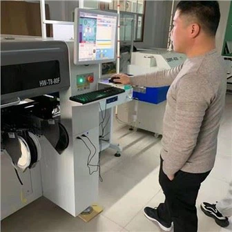
Pick-and-place: A programmable machine with a robotic arm that picks components from an automatic feeder, moves them to a fixed point on the PCB, and places them in the correct location in the correct orientation .
Placement equipment: a machine that combines high speed and accurate positioning to place components on a PCB, divided into three types: mass transfer of SMD, X/Y positioning and in-line transfer systems, which can be combined to fit components into circuits board design.
starts with the letter R
Reflow soldering: The process of placing surface mount components into solder paste for permanent connection through various stages including: preheating, stabilization/drying, reflow peaking, and cooling.
Repair: The action of restoring the functionality of a defective assembly.
Repeatability: The ability of the process to accurately return to a characteristic target. A metric to evaluate processing equipment and its continuity.
Rework: An iterative process of bringing an incorrect assembly back into compliance with specification or contract requirements.
Rheology: Describes the flow of a liquid, or its viscosity and surface tension properties, eg, solder paste.
(S~Z)
Begins with the letter S
Saponifier: An aqueous solution of organic or inorganic main ingredients and additives used to facilitate the removal of rosin and water-soluble fluxes by, for example, dispersible cleaners.
Schematic: A diagram that uses symbols to represent a circuit arrangement, including electrical connections, components, and functions.
Semi-aqueous cleaning: A technique involving solvent cleaning, hot water flushing, and drying cycles.
Shadowing: In infrared reflow soldering, the body of the component blocks energy from certain areas, resulting in a phenomenon where the temperature is not high enough to completely melt the solder paste.
Silver chromate test: A qualitative, examination of the presence of halide ions in RMA flux. (RMA reliability, maintainability and availability)
Slump: The diffusion of solder paste, glue and other materials before curing after stencil screen printing.
Solder bump (solder ball): The ball-shaped solder material is bonded to the contact area of passive or active components, and plays the role of connecting with the circuit pad.
Solderability: The ability of a conductor (pin, pad or trace) to wet (become solderable) in order to form a strong connection.
Soldermask: A processing technique for a printed circuit board in which all surfaces except the connection points to be soldered are covered with a plastic coating.
Solids: In the flux formulation, the weight percentage of rosin, (solid content)
Solidus: The temperature at which the solder alloy of some components begins to melt (liquefy).
Statistical process control (SPC): The use of statistical techniques to analyze process output and its results to guide actions, adjust and/or maintain a state of quality control.
Storage life: The time during which the glue is stored and remains useful.
Subtractive process: By removing the conductive metal foil or cover